W803-Pico Getting Started Guide
Preparation
W803-Pico Development Board
Type-C Data Cable
USB convert to serial drive(Click to download the CH34X driver)
PC (Windows, or Linux)
You can skip the introductory section and go directly to the Application Development section.
Overview
The W803-Pico is a development board based on Winner Micro W803 chip as its main controller, which supports IEEE802.11 b/g/n Wi-Fi and BT/BLE4.2 protocol Bluetooth. It has a built-in high performance 32-bit processor with 240MHz, 2MB Flash and 288KB RAM, DIP package, PCB antenna.With a rich set of interfaces, it is simple to use. W803-Pico development board mainly integrates the following peripheral devices:
External PCB antenna
Integrated 5v to 3.3v LDO chip
Provides BOOT, RESET button
Built-in power indicator (PWR), user indicator (LED) light
This greatly reduces the number and cost of additional purchases and installation of these components by the user, as well as the complexity of additional assembly and testing, and increases usability.
In order to facilitate customers to connect more peripherals, all the IO signals and system power pins on the W803-Pico are led through the pins below and above the development board, allowing customers to plug the W803-Pico directly into other development boards or use DuPont cables to connect to other peripherals for use, which greatly increases the diversity of use for users.
Hardware Specifications
The main components of the W803-Pico development board are illustrated below.
The hardware specifications of the W803-Pico development board are described in the following table.
Hardware Interface |
Power Supply |
5V DC |
LEDs |
Power Supply Indicator (PWR), User Indicator (LED) |
|
USB Interface |
Type-C |
|
Keypad |
BOOT, RESET |
|
External Dimensions |
Dimensions (L*W*H) |
52.7*21.0*4.95mm |
Temperature Range |
Operating Temperature |
-40°C~85°C |
Storage Temperature |
-40°C~85°C |
|
MCU Characteristics |
CPU |
32-bit XT804 processor with 240MHz operating frequency |
Memory |
2MB Flash, 288KB RAM |
|
Security Features |
Security Engine |
Tee Security Engine, with Code to Distinguish Between Secure and Non-secure Worlds |
Security Features |
Firmware Signature, Firmware Encryption |
|
Wi-Fi Features |
Protocols |
IEEE802.11 b/g/n. |
Bandwidth Operating Mode |
20M/40M |
|
Encryption Method |
WMM/WMM-PS/WPA/WPA2/WPS |
|
Operating Mode |
Station, Soft-AP, Soft-AP/Station |
|
Bluetooth Characteristics |
Protocols |
BT/BLE4.2 protocol support |
Operating Mode |
Supports BT/BLE dual-mode operation |
Power Options
The development board can choose either of the following two power supply modes:
VBUS Power Supply, from USB 5V supply.
VSYS Power Supply, directly connected to the W803 chip, 3.3V supply.
Warning
The above power supply modes may not be connected at the same time, otherwise the development board or power supply may be damaged.
Working Conditions
The operating conditions of the W803-Pico development board are shown in the following table.
Attributes |
Parameters |
Type-C USB Input Voltage |
DC 5V(+/- 10%) |
Operating Temperature |
-40°C~85°C |
Pin Description
The following table describes the names and functions of the development board’s I/O pins, see the Development Board Pinout, Schematic and Layout Diagram section for the exact layout
No. |
Name |
Type |
Multiplexing Function |
Maximum Frequency |
Pull-up and pull-down capability |
Driving capacity |
1 |
PB0 |
I/O |
PWM0/LSPI_MISO/UART3_TX/PSRAM_CK/Touch_3 |
80MHz |
UP/DOWN |
12mA |
2 |
PB1 |
I/O |
PWM1/LSPI_CK/UART3_RX/PSRAM_CS/Touch_4 |
80MHz |
UP/DOWN |
|
3 |
GND |
P |
||||
4 |
PB2 |
I/O |
PWM2/LSPI_CK/UART2_TX/PSRAM_D0/Touch_5 |
80MHz |
UP/DOWN |
12mA |
5 |
PB5 |
I/O |
LSPI_MOSI/UART2_CTS/UART4_RX/PSRAM_D3/Touch_8 |
80MHz |
UP/DOWN |
12mA |
6 |
PB3 |
I/O |
PWM3/LSPI_MISO/UART2_RX/PSRAM_D1/Touch_6 |
80MHz |
UP/DOWN |
12mA |
7 |
PB4 |
I/O |
LSPI_CS/UART2_RTS/UART4_TX/PSRAM_D2/Touch_7 |
80MHz |
UP/DOWN |
12mA |
8 |
GND |
P |
||||
9 |
PA4 |
I/O |
JTAG_SWO/I²C_SDA/PWM4/I²S_BCK/ADC1 |
20MHz |
UP/DOWN |
12mA |
10 |
PA1 |
I/O |
JTAG_CK/I²C_SCL/PWM3/I²S_LRCK/ADC0 |
20MHz |
UP/DOWN |
12mA |
11 |
PB6 |
I/O |
UART1_TX/MMC_CLK/HSPI_CK/SDIO_CK/Touch_9 |
50MHz |
UP/DOWN |
12mA |
12 |
PB7 |
I/O |
UART1_RX/MMC_CMD/HSPI_INT/SDIO_CMD/Touch_10 |
50MHz |
UP/DOWN |
12mA |
13 |
GND |
P |
||||
14 |
PB6 |
I/O |
UART1_TX/MMC_CLK/HSPI_CK/SDIO_CK/Touch_9 |
50MHz |
UP/DOWN |
12mA |
15 |
PB11 |
I/O |
I²S_DO/MMC_D3/HSPI_DO/SDIO_D3 |
50MHz |
UP/DOWN |
12mA |
16 |
PB10 |
I/O |
I2S_DI/MMC_D2/HSPI_DI/SDIO_D2 |
50MHz |
UP/DOWN |
12mA |
17 |
PB9 |
I/O |
I²S_LRCK/MMC_D1/HSPI_CS/SDIO_D1/Touch_12 |
50MHz |
UP/DOWN |
12mA |
18 |
WAKEUP |
I |
||||
19 |
PA14 |
I/O |
TOUCH_CAP(CDC)/UART5_CTS/PWM4 |
50MHz |
UP/DOWN |
12mA |
20 |
PB8 |
I/O |
I²S_BCK/MMC_D0/PWM_BREAK/SDIO_D0/Touch_11 |
50MHz |
UP/DOWN |
12mA |
21 |
BOOT |
I |
||||
22 |
GND |
P |
||||
23 |
PA12 |
I/O |
TOUCH_CAP(CMOD)/UART5_TX/PWM2 |
50MHz |
UP/DOWN |
12mA |
24 |
RESET |
I |
||||
25 |
PA7 |
I/O |
PWM4/LSPI_MOSI/I²S_MCK/I²S_DI |
25MHz |
UP/DOWN |
12mA |
26 |
PA4 |
I/O |
JTAG_SWO/I²C_SDA/PWM4/I²S_BCK/ADC_1 |
20MHz |
UP/DOWN |
12mA |
27 |
GND |
P |
||||
Notes: |
ADC_VREF is the ADC calibration voltage, 3.3V typical. |
|||||
USB connection to serial port 0 for firmware burning, AT command interaction, etc. |
Application Development
Before powering up the W803-Pico, first make sure the development board is intact.
Now, go to the Building the compiling environment section in the Quick Start to see how to set up the development environment and try to burn the sample project to your development board.
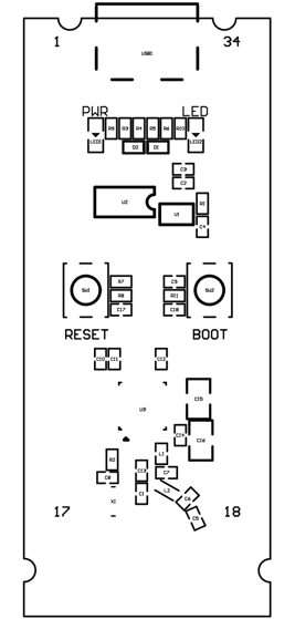
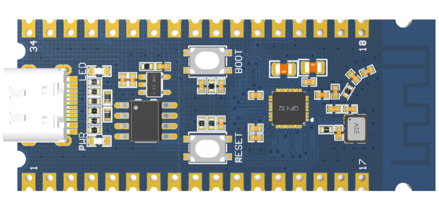
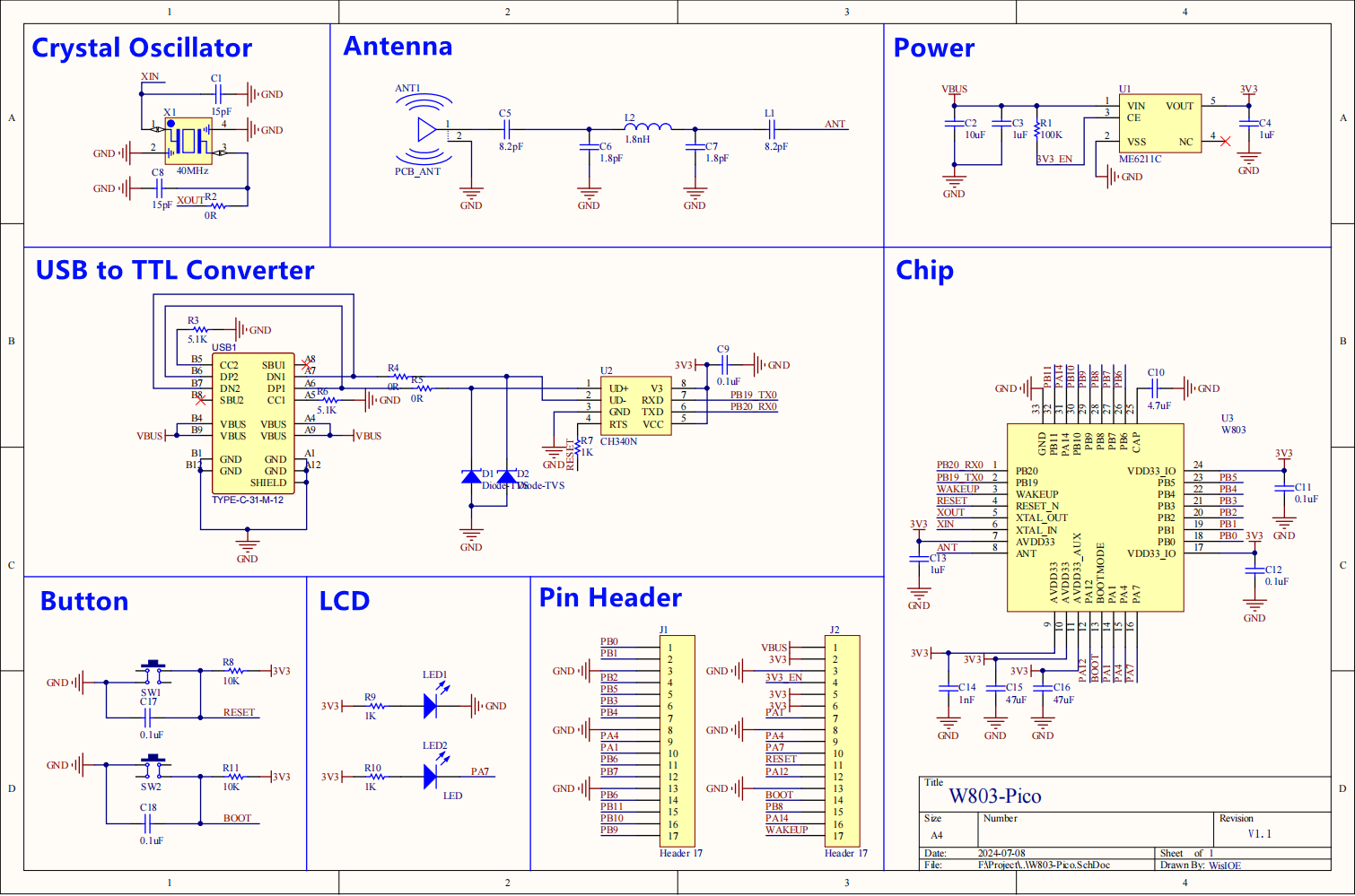
Development Board Pinout, Schematic and Layout Diagrams
The pinout of the W803-Pico development board is shown below.

The schematic diagram of the W803-Pico development board is shown below.
The layout of the W803-Pico development board is shown below.